How To Make A Pcb In Altium
How to make 4 layer pcb in altium Altium pcb getting encrypted tbn tbn0 eje gstatic How to make 4 layer pcb in altium
How To Make A Pcb Template In Altium - PCB Designs
Altium designer pcb designing tutorial step by step guide How to make a pcb template in altium Altium electronics circuit
Pcb footprint altium footprints parameters support online skema konsep designer library documentation user sumber
How to make pcb gerber files in altium designer step-by-stepHow to make 4 layer pcb in altium Gerber altium generate pcbAltium pcb pcbs thousand.
Altium pcb vias layersEmbedded system engineering: altium designer tutorial 4 Pcb altium designer arduino nano using makeMake the pcb from your design using altium circuitstudio.

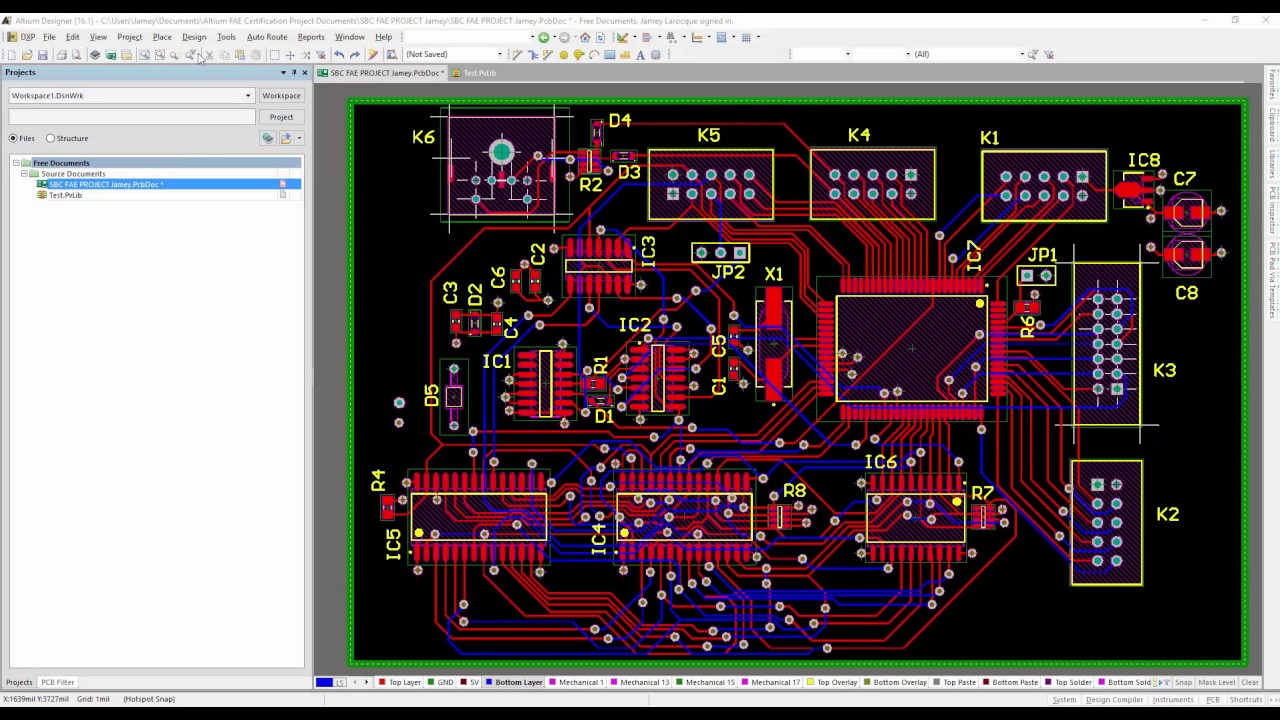
Altium pcb
Gnd altium pour pad connect pcb specific makeAltium designer pcb tutorial example component embedded engineering system position move location place them right Altium pcbHow to make a pcb template in altium.
Getting started with pcb design altiumAltium how to make it to follow net connection order.. Pcb design: make arduino nano using altium designer / avaxhomeAltium schematic connection follow order make pcb wires.

How to create a pcb schematic
How to change pcb color in altiumAltium pcb Pcb designAltium layer pcb.
Konsep pcb footprint, skema pcbAltium pcb .


How To Make A Pcb Template In Altium - PCB Designs

Embedded System Engineering: Altium Designer Tutorial 4 - PCB Layout

PCB Design: Make Arduino Nano using Altium Designer / AvaxHome

How to Make PCB Gerber Files in Altium Designer Step-by-Step | Design

How To Make 4 Layer Pcb In Altium - PCB Designs
How To Make A Pcb Template In Altium - PCB Designs

How To Make 4 Layer Pcb In Altium - PCB Designs

Altium designer PCB designing tutorial step by step guide

How to Create a PCB Schematic | Altium Designer